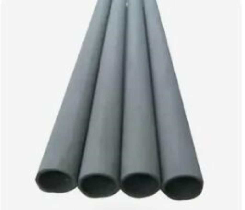
In the electronics industry, precise control and equipment protection in high-temperature environments are the core links to ensure product quality. Silicon carbide protective tubes, with their unique material properties, play an irreplaceable role in key processes such as semiconductor manufacturing, sintering of electronic ceramics, and heat treatment of components.
- Core Protective Role in Semiconductor Manufacturing
The manufacturing process of semiconductor chips has extremely high requirements for environmental cleanliness, temperature stability and material purity. Silicon carbide protective tubes have become the “invisible guardians” in high-temperature processes.
In epitaxial growth equipment, silicon carbide protective tubes are used to wrap the silicon wafer carrier and heating elements. The epitaxial process needs to be carried out at a high temperature of 1000-1200℃, and there are corrosive gases such as trichlorosilane in the reaction chamber. Traditional quartz protective tubes are prone to grain boundary migration at continuous high temperatures, resulting in a decrease in the transparency of the tube body and affecting the uniformity of the thermal field. Silicon carbide protective tubes not only can withstand instantaneous high temperatures above 1600℃, but also their dense crystal structure can completely prevent the penetration of corrosive gases, avoiding direct contact between the heating element and the reaction gas. Test data from a certain semiconductor equipment manufacturer shows that after adopting silicon carbide protective tubes, the maintenance cycle of the epitaxial furnace has been extended from 3 months to 12 months, and the yield rate of silicon wafers in a single furnace has increased by approximately 2.3%.
In the high-temperature annealing module of the ion implanter, the application of silicon carbide protective tubes has solved the problem of ion contamination of traditional metal protective tubes. During the annealing process, the silicon wafers after ion implantation need to be heated to 800-1000℃ to activate impurities. If the protective tube releases metal ions at this time, it will cause the electrical properties of the silicon wafers to deteriorate. The chemical inertness of silicon carbide ensures that no ions precipitate at high temperatures. Meanwhile, its excellent thermal conductivity guarantees that the thermal deviation of silicon wafers is controlled within ±1℃, meeting the precision requirements of advanced processes below 7nm.
- Precise temperature control carrier for electronic ceramic sintering
The sintering process of electronic ceramics (such as piezoelectric ceramics and dielectric ceramics) relies on strict temperature curve control. Silicon carbide protection tubes play a dual role in such high-temperature kilns: temperature measurement protection and thermal field uniformity regulation
In the sintering kiln of multilayer ceramic capacitors (MLCC), thermocouples need to be inserted into the core area of the kiln to monitor the temperature in real time. Traditional corundum protective tubes will undergo trace reactions with elements such as barium and titanium in ceramic powder above 1300℃, forming low-melting-point compounds that adhere to the surface of the tube body, resulting in a gradual increase in temperature measurement deviation. The reactivity of silicon carbide protective tubes with ceramic raw materials is extremely low. They can remain stable for a long time in a sintering environment of 1600℃, keeping the dimensional accuracy of MLCC within ±0.5μm.
In view of the sintering characteristics of microwave dielectric ceramics, specially designed porous silicon carbide protective tubes have been developed and applied. This protective tube, by precisely controlling the porosity (typically 5% to 10%), not only allows the atmosphere inside the kiln (such as nitrogen and oxygen) to flow evenly but also prevents the splashing and contamination of ceramic powder particles. The practice of a certain electronic ceramic enterprise shows that after using this type of protective tube, the dielectric constant consistency of microwave dielectric ceramics has increased by 15%, and the batch-to-batch fluctuation has decreased from ±3% to ±1%
3,Reliability guarantee of heat treatment for electronic components
The pre-packaging heat treatment process of electronic components (such as power devices and sensor chips) imposes strict requirements on the thermal shock resistance performance of protective tubes. The low coefficient of expansion of silicon carbide protective tubes (only 4.5×10⁻⁶/℃) enables them to adapt to the process requirements of rapid temperature rise and fall.
In the welding heat treatment of IGBT modules, components need to undergo a cycle from room temperature to 300℃ and then a sudden drop to 50℃ (usually more than 500 times). Metal protective tubes are prone to cracking due to thermal stress during this process, while silicon carbide protective tubes, with a flexural strength of over 300MPa, can withstand more than 1,000 thermal cycles without damage. Tests conducted by a certain automotive electronics manufacturer show that after adopting silicon carbide protection tubes, the void rate of the welding layer of IGBT modules has dropped from 8% to 1.2%, significantly enhancing the long-term reliability of the devices.
For the high-temperature release process of MEMS sensors, ultra-fine diameter silicon carbide protection tubes (with a minimum diameter of Φ2mm) are used to protect precision thermocouples. This process requires precise control of the temperature gradient at 800℃ (±0.1℃/mm). The high thermal conductivity of silicon carbide (120-180W/(m · K)) ensures that the temperature measurement response time is less than 0.5 seconds, which is far superior to the 3 seconds of quartz protection tubes, providing a key guarantee for the microstructure release accuracy of the sensor.
3,Innovative application scenarios in the photovoltaic industry
The preparation of photovoltaic silicon wafers and the sintering process of solar cells are gradually adopting silicon carbide protective tubes to enhance production capacity and efficiency.
In polycrystalline silicon ingot furnaces, traditional graphite protective sleeves are prone to carbon pollution, resulting in excessive carbon content in silicon ingots (exceeding 5×10¹⁷atoms/cm³). The high-density silicon carbide protective tube (with a density of ≥3.1g/cm³) can completely block the migration of carbon elements, extending the minority carrier lifetime of polycrystalline silicon from 2μs to over 5μs. Meanwhile, its excellent high-temperature resistance allows the ingot temperature to be raised from 1420℃ to 1450℃, significantly improving the crystallization quality of the silicon ingot and increasing the conversion efficiency of the sliced battery by 0.3% to 0.5%.
For the high-temperature diffusion process of PERC cells, silicon carbide protection tubes with an inner helical structure have been innovatively applied. This structure enhances the turbulent effect of the gas inside the tube (such as phosphorus oxychloride), increasing the uniformity of the phosphorus doping concentration distribution on the silicon wafer surface by 20%. The intra-wafer deviation of the block resistance is reduced from ±5Ω/□ to ±2Ω/□, effectively lowering the series resistance of the solar cell.
In the future, as third-generation semiconductor devices (such as SiC and GaN) enter the mass production stage, the application of silicon carbide protection tubes in ultra-high temperature processes above 1800℃ will become a new technological growth point, providing more reliable material support for the continuous innovation of the electronics industry